- Home
- All Courses
- Best CMOS & FPGA Design Flow Training in Delhi
Best CMOS & FPGA Design Flow Training in Delhi & Best CMOS & FPGA Design Flow Training Institute in Delhi
 4.9
4.9
out of
5
based on
9759user reviews.
Join Best CMOS & FPGA Design Flow Training in Delhi, CMOS & FPGA Design Flow Course in Delhi, CMOS & FPGA Design Flow Institute in Delhi
APTRON Delhi offers an inclusive CMOS & FPGA Design Flow training in delhi. The extensive practical training provided by CMOS & FPGA Design Flow training institute in delhi equips live projects and simulations. Such detailed CMOS & FPGA Design Flow course has helped our students secure job in various MNCs. The trainers at APTRON Delhi are subject specialist corporate professionals providing in-depth study in CMOS & FPGA Design Flow course in delhi. Participants completing the CMOS & FPGA Design Flow certification have plethora of job opportunities in the industry.
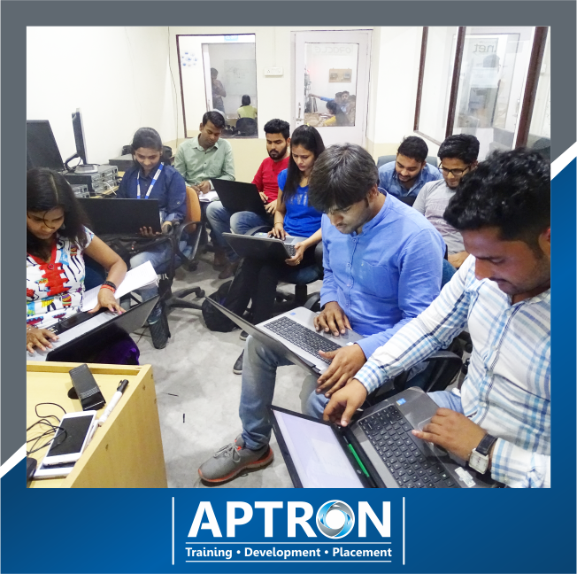
Further, we have kept the CMOS & FPGA Design Flow course in delhi duration flexible. From online classroom to fast-track & one-to-one classroom CMOS & FPGA Design Flow training is provided during weekdays and weekends to the attendees. Our modern lab is equipped with latest technologies helping students avail a successful CMOS & FPGA Design Flow training and certification from the institute.
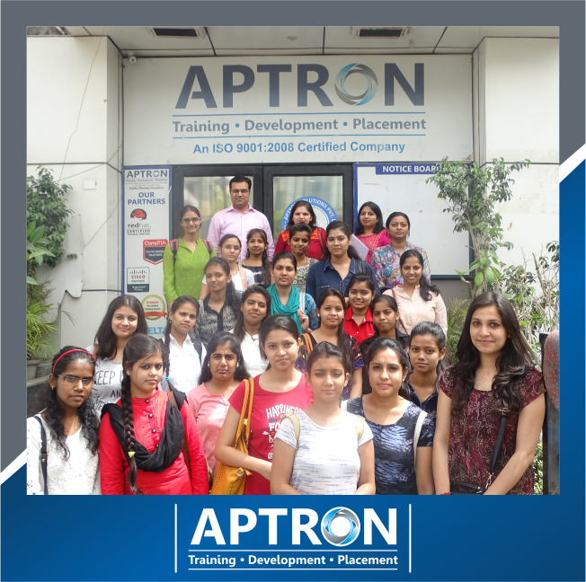
APTRON Delhi, recognized among the top ten CMOS & FPGA Design Flow training institute in delhi, has training module for beginners, intermediates, and experts. Whether you are a college student, I.T professional or a project manager; the best CMOS & FPGA Design Flow training institute in delhi offers best training environment, veteran CMOS & FPGA Design Flow trainers, and flexible training schedules for entire modules. Also, the best training institute for CMOS & FPGA Design Flow training in delhi asks for a value to money fee from the students. The pocket-friendly CMOS & FPGA Design Flow course fee structure can be afford by students coming from all walks of life.
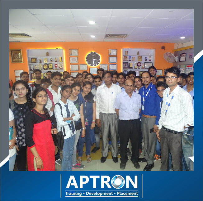
After CMOS & FPGA Design Flow course in delhi, learning the interview skills indeed becomes mandatory. Along with CMOS & FPGA Design Flow classes in delhi, we have sessions for personality development, spoken English, and presentation. At our CMOS & FPGA Design Flow training centre in delhi, Placement team schedules recruitment drives where the technology-driven branded companies hand-pick our students. CMOS & FPGA Design Flow training in delhi with placement assistance is the key feature which rated us 'star five' in the reviews by our aspirants. Reviews and honest feedback is mentioned on our official website. APTRON Delhi is one of the best CMOS & FPGA Design Flow training centres in delhi delivering out-of-box thinking professionals to the industry.
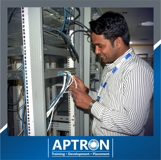
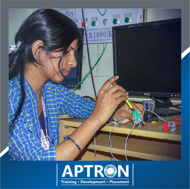
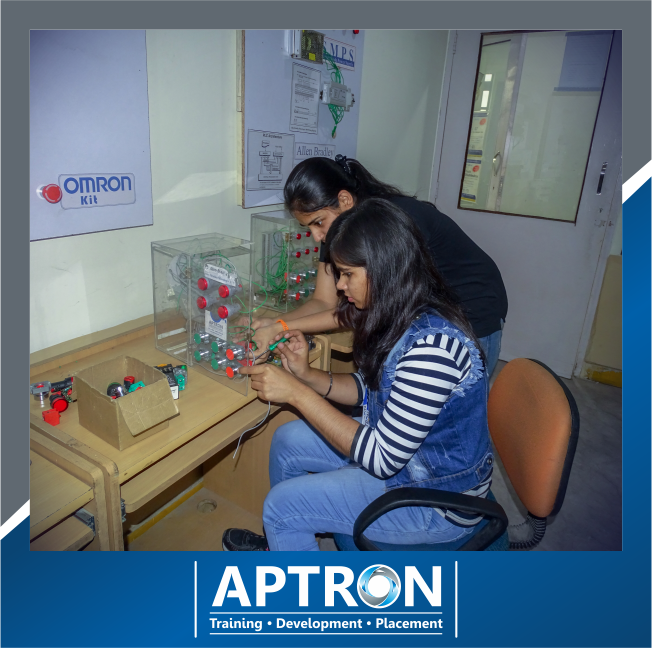
APTRON Delhi has a modern lab equipped with latest devices that facilitate participants in having a thorough hands-on experience through live projects. Such training in delhi boost the confidence level in participants to face the real-time challenges successfully in a job.
The CMOS & FPGA Design Flow syllabus includes for CMOS & FPGA Design Flow course module on real time projects along with placement assistance. CMOS & FPGA Design Flow topics covered are
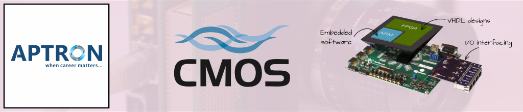
Introduction to VLSI CMOS, Characterization of CMOS Circuits, Layout Representation for CMOS Circuits, Architecture based coding, Back annotation, Gate level simulation, SDF Format,False paths and multi cycle paths
& Many more. Check the duration, course content and syllabus given below.
CMOS & FPGA Design Flow Course Fee and Duration
| Track |
Regular Track |
Weekend Track |
Fast Track |
| Course Duration |
45 - 60 Days |
8 Weekends |
5 Days |
| Hours |
2 hours a day |
3 hours a day |
6+ hours a day |
| Training Mode |
Live Classroom |
Live Classroom |
Live Classroom |
Course Content and Syllabus for CMOS & FPGA Design Flow Training in Delhi
CMOS & FPGA Design Flow Course Contents
- Introduction to VLSI CMOS
- CMOS Fundamentals and Characterization
- NMOS/PMOS/CMOS Technologies
- Fabrication Principles
- Different Styles of Fabrication for NMOS/PMOS/CMOS
- Design with CMOS Gates
- Characterization of CMOS Circuits
- Scaling Effects
- Sub-Micron Designs
- Parasitic Extraction and Calculations
- Subsystem Design
- Layout Representation for CMOS Circuits
- Design Exercise using CMOS
- Introduction of IC Design
- Different Methodologies for IC Design
- Fabrication Flows and Fundamentals
FPGA Flow
- Re-configurable Devices, FPGA’s/CPLD’s
- Architectures of XILINX, ALTERA Devices
- Designing with FPGAs
- FPGA’s and its Design Flows
- Architecture based coding
- Efficient resource utilization
- Constrains based synthesis
- False paths and multi cycle paths
- UCF file creation
- Timing analysis/Floor Planning
- Place and route/RPM
- Back annotation, Gate level simulation, SDF Format
- DSP on FPGA
- Writing Scripts
- Hands on experience with industry Standard Tools
- ASIC Flow
Project Software Package
Top 20 Reasons to Choose APTRON for CMOS & FPGA Design Flow Training in Delhi
- Our CMOS & FPGA Design Flow training in Delhi is developed in compliance to current IT industry.
- We provide the best CMOS & FPGA Design Flow training in Delhi covering entire course modules during the CMOS & FPGA Design Flow classes. Also, students avail CMOS & FPGA Design Flow course in Delhi with placement assistance.
- CMOS & FPGA Design Flow training in Delhi are scheduled on weekdays and weekends. Also students can opt for customized schedule according to the requirements.
- Our team of trainers are industry-experts possessing more than a decade experience in training.
- Mentors coaching CMOS & FPGA Design Flow training in Delhi not only help students in accomplishing live projects, but also provide session on interview preparation along with placement assistance.
- Ultra-modern I.T laboratory equipped with latest infrastructure.
- Our lab is open 365 days in a year. Students, according to their convenience can utilize the lab for completing projects and practice the technical assignments.
- Our training classrooms are equipped with modern I.T infrastructure such as projectors, live racks, Wi-Fi, and digital pads.
- We facilitate our students with glass-door study room and discussion zone area (meeting room) to enhance their learning and exploring abilities.
- Along with technical training and course, we organize no cost sessions on personality development spoken English, group discussion, mock interview and presentation skills to develop high level of confidence in students.
- We also organize no cost personality development and presentation seminars.
- Our course material includes books, and soft copies of tutorials in the form of PDFs, sample papers, technical and HR interview questions, and projects available on our website.
- Students enrolled to CMOS & FPGA Design Flow training in Delhi can also avail hostel facility at Rs.4,500/- a month.
- We facilitate students with no cost study material, soft copies of PDFs, video training, sample questions for respective certification, and interview questions along with lab guides made available on our website for quick access.
- Our certificates are globally recognized provided after completion of course.
- We facilitate students with Extra Time Slots (E.T.S) for doing unlimited practical at no cost.
- According to the requirements, students can retake the class at no cost.
- Our instructors pay one-to-one attention.
- To enhance knowledge of the students, the complex technical concepts are imparted through easy coaching.
- We accept master and visa cards (Debit & Credit), also payment mode cash, cheque, and Net Banking available.
APTRON Delhi Trainer's Profile for CMOS & FPGA Design Flow Training in Delhi
APTRON's Delhi CMOS & FPGA Design Flow Trainers are:
- Our trainers are industry-experts and subject specialists who have mastered on running applications providing best CMOS & FPGA Design Flow training to the students.
- We have received various prestigious awards by our recognized IT partners and organizations.
- Our trainers are MNC working professionals employed in HCL Technologies, Birla-soft, TCS, IBM, Sapient, Agilent Technologies, and so on.
- Our trainers are certified professionals possessing 7+ years of experience in the industry.
- Our trainers have regular coordination with MNCs HR team on daily basis.
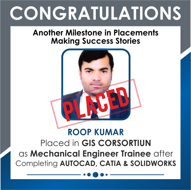
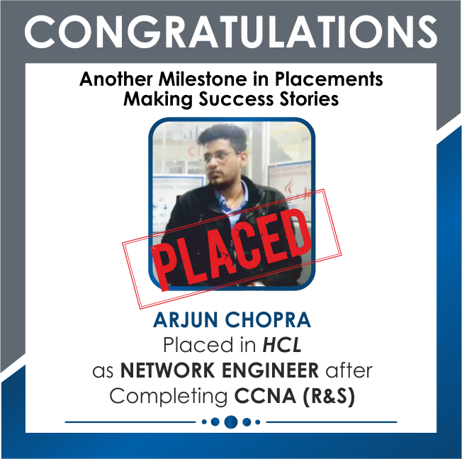
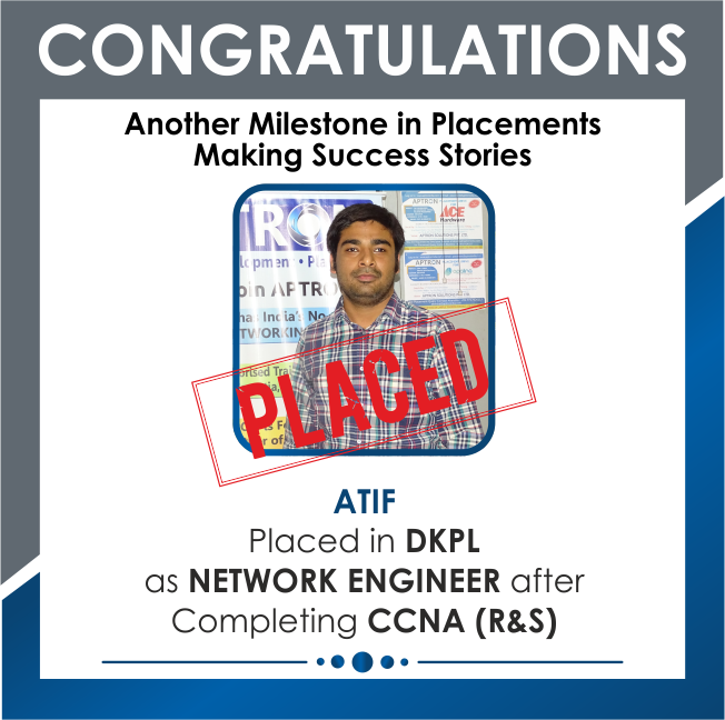
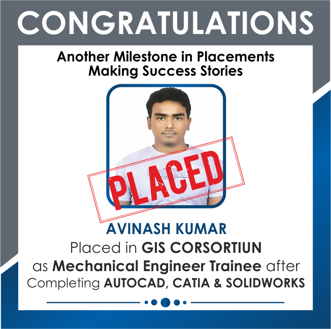
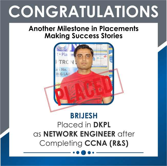
Placement Assistance after CMOS & FPGA Design Flow Training in Delhi
Along with CMOS & FPGA Design Flow training in Delhi, we provide placement assistance to the students.
- APTRON Delhi with successful 96% placement rate has a dedicated HR wing that assist students in securing placement according to their requirements.
- APTRON Delhi assist students in developing their resume matching the current industry needs.
- APTRON Delhi, apart from course training, also facilitate students with sessions provided on personality development, spoken English, group discussion, mock interview, and presentation skills to develop a high level of confidence for facing tricky and challenging interviews competently.
- APTRON Delhi provide an in-depth training to the students, which assist them to secure placement in top IT firms such as HCL, TCS, Infosys, Wipro, Accenture, and many more effortlessly.